Designing Circuit Boards
Creating a PCB layout in HiWIRE® is fairly straight forward. You load components from a library and connect them with lines. You've already seen enough to do simple designs
However, HiWIRE® includes facilities that can make your work much easier, including trace ratsnesting (to assist in manual placement and routing), connection and design-rule checking, automatic drill-tape generation, etc.
To use these facilities, HiWIRE® expects your drawing to conform to a well-defined set of conventions. These conventions are similar to those you saw with schematics, but there are differences.
Definitions
An electronic system is a collection of interconnected components; each component has two or more terminals or pins. These pins are interconnected with other pins to form nodes or nets.
In a circuit-board layout, each component is represented by a footprint. The terminals are represented by pads; interconnections by traces. “Represented” may be an understatement, since the drawing is normally an exact likeness of the layout used to manufacture the circuit board.
Before discussing HiWIRE's drawing conventions for PCBs, here are some terms we'll use in the discussion.
- conducting layer
A drawing layer on which electrical connections may be made. The number of conducting layers you'll use depends in part on the complexity of your design and the number of physical layers you need to realize it. For a typical two-layer board, HiWIRE layers 0, 1 and 2 are conducting layers. By convention, conducting layers start at 0 and count upward.
- insulating layer
A drawing layer greater than the maximum conducting layer. By convention, insulating layers start at 255 and count downward.
- conductor
A solid line, pad, polygon or arc on a conducting layer of your drawing. Dotted, dashed and zero-width lines are not conductors.
- trace
A conductor (usually a line) that connects component pins (usually pads).
- site label
A label with an attribute of site. Note that site must be spelled exactly as shown, in lower-case letters. It won't do to use Site or SITE. Site labels may be placed on any layer, and associate a group of drawing objects with a particular component. Labels with attributes, including site labels, cannot be conductor labels.
- conductor label
A label without an attribute on a conducting layer whose hotspot lies inside a conductor on that layer.
- drawing component
A group of objects that includes a site label. Although the drawing component can contain nested groups, the site label must be outside all nested groups. Drawing components correspond to the actual components in your design. When it is clear we are referring to a drawing component, and not a real component, we may shorten the name to “component”.
- footprint
A drawing component in a circuit board layout that does not contain any nested drawing components. In a PCB layout, footprints are the pads or traces soldered or otherwise connected to the physical pins of the real component.
Layering rules for conductors and conductor labels are stricter for PCBs than for schematics. Specifically:
The conductor label must be on the same layer as the conductor or on layer 0. (In schematics, the conductor and its label could be on any conducting layer.)
The conductor must be a member of the same group (or some nested group) as the label. A label in a group cannot reach outside the group to touch a conductor. However, it can reach inside groups, even inside nested groups, to touch conductors there.
Layout Conventions
A circuit-board layout will normally use several drawing layers. These drawing layers will be combined in special ways to create the artwork for the physical layers of your board.
Although you can use virtually any layer for any purpose, the HiWIRE footprint libraries and supplied Python scripts assume the following conventions:
- 244, 245
Interior ground plane for multi-layer boards. 244 is an additive layer; objects here define where copper is added to form connections between component pins and the plane. 245 is a subtractive layer; objects on this layer describe where copper is removed to form insulating gaps.
- 246, 247
Interior power plane for multi-layer boards. 245 is additive; 247 is subtractive.
- 248, 249
Paste mask layers. Objects on these layers define where a solder suspension is applied to your board. This solder is later melted during reflow soldering to connect surface-mount components to their mounting pads. Layer 249 is for normal, top-mounted components; layer 248 is for the occasional component mounted to the bottom of your board.
- 250, 251
Solder mask. An insulating coating is often laminated on the top and bottom surfaces of a circuit board to retard the growth of solder whiskers and facilitate wave soldering. Objects on this layer define where the underlying conductors are exposed to the surface to allow them to be soldered. Layer 250 is for the bottom; 251 is for the top of the board.
- 252
CNC milling machine paths. Lines on this layer describe the path taken by a CNC milling machine as it cuts the outline of your board and separates it from the web of excess material used during manufacture.
- 253
CNC drilled holes. Round pads on this layer describe any holes drilled in your board for mounting or to accomodate through-hole components.
- 254, 255
Silkscreens. Objects on this layer define where non-conducting ink is applied to your board to aid in assembly or field repair. Layer 255 is for the top of the board; layer 254 is reserved in case you want to place annotation on the bottom.
- 0
All-layer pads and vias for through-hole components and conductors that are present on all physical layers.
- 1, 3, 5, …
Solder-side (bottom) signal layers. Lower-numbered layers are closer to the surface; higher-numbered layers are buried underneath.
- 2, 4, 6, …
Component-side (top) signal layers. Lower numbered layers are closer to the surface.
Examples
A single-layer board might use only layer 0 for conductors (along with layer 255 if silkscreen annotation was required). A double-sided board would use layers 0, 1 and 2 for conductors. A six-layer board that included a power and ground plane would use layers 0 through 4 for the four signal layers and 244 through 247 for the power/ground planes.
Consider the simple 8-pin DIP footprint shown below:
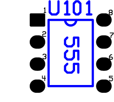 |
Figure 11A |
On layer 0 (here rendered in black), it has eight pads accompanied by eight conductor labels that define the pins of the footprint. The labels are normally much smaller, but here are enlarged for clarity.
A four-segment line, a 180-degree arc, a part label 555, and a site label U101 on layer 255 (rendered in blue) form a pictorial representation of the actual component that is suitable for a silkscreen.
Connecting with Traces and Vias
In PCB layout, HiWIRE considers two conductors to be connected if any part of one touches the other and either:
Both are on the same layer, –or–
One is on layer 0.
Layer 0 is all layers, so one might consider these two conditions to be equivalent.
Unlike schematic wires, traces and pads are not insulated; any contact confers a connection. The only way two traces can cross without connecting is if they are on different layers.
A via forms a connection between layers of a circuit board. The most common type of via is an all-layer via. It consists of pads on each physical layer interconnected by plating the wall of the hole drilled though their center. In HiWIRE, it is easiest to use a layer-0 pad to represent an all-layer via.
Other types of vias include blind and buried vias. These vias interconnect two or more adjacent copper layers which may be interior to the surface of the board. The via is buried if it does not connect to an exterior layer; blind if it does.
Blind and buried vias that exist only on a subset of the physical layers are represented in the layout by a stack of separate conductors (typically pads) on their respective layers. A conductor label on layer 0 (all layers) connects these pads regardless of their layer. These via-stitching labels should be grouped with their pads to keep them from forming connections with other, unrelated conductors. The text of the label is unimportant (e.g., all conductor stitches may use labels with a text part of X), but the label hotspot must be inside all the pads in the stack.
In the following example, you see four pads on layer 0 (in black). The first and third are connected by a five-segment trace on layer 2 (in green); the first and second are connected by traces on layers 1 (in red) and 2 and stitched together by a layer-0 conductor label, X (here enlarged for clarity).
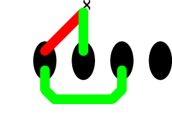 |
Figure 11B |
Using Labels to Name Conductors
HiWIRE uses the same rules to generate names for circuit-board components and pins as it does for schematics.
In a circuit-board layout, you can name both pads and traces using a conductor label, but only inside a component footprint. Outside this restricted zone, conductor labels can act as stitches, but they do not name the conductors they connect.
In the example below, two pads of the footprint for U605 are interconnected by a three-segment trace.
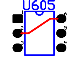 |
Figure 11C |
There are three conductors in the net: the 3-segment trace and the two pads of the footprint. If asked to describe the interconnections made by net, HiWIRE would respond a list of its conductor names:
( (U605 2) (U605 6) )
Two conductors with the same name are connected, even if they do not touch. For example, If you have two pads names G2 in the same footprint, HiWIRE will assume they are electrically connected.
Note, however, that while they are are conductor labels by definition, conductor stitches do not name their conductors unless they are contained in a footprint.
Summary of Connection Rules
In circuit-board layout, conductors may be connected by any of three means:
By virtue of a physical connection
Because a (layer-0) conductor label hotspot touches both conductors
By having the same name
Defining Component Footprints
Often, the easiest way to create a new footprint is to modify an existing one from HiWIRE's library. For example, the footprint for an SPDT reed rrelay in a DIP package on the right was made quickly by Edit->Freeing, deleting a few unneeded pins, and Edit->Binding it back.
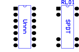 |
Figure 11D |
Starting from Scratch
To define a component footprint without modifying an existing one:
In the preferences dialog:
Set the grid spacing to a convenient factor of the pin spacing. For example, if your conenctor has pins arranged in a 2x25 array on 0.1-inch centers, a spacing of 50 or 100 mils works nicely.
Set the pad size and shape to the one recommended by the manufacturer.
Set the text size to creat a conductor label small enough not to get in the way when you're working on the board. These conductor labels won't appear in your prints or photoplots; the HiWIRE library uses size-6 labels for most of its footprints.
Change to the layer occupied by the footprint conductors. For through-hole components this is layer 0; for surface-mount use layer 2.
Drag in pads, and lay out the footprint as recommended in the component data sheet. Don't forget to leverage your work.
Drag in an emryonic label and copy it as many times as required to name all the conductors. You can plop the labels into the center of their pad if you don't think you'll need to see them. Otherwise you can keep Shift depressed and carefully locate them near the edge of the pad.
Go back and change the embryonic Txt in each label to the correct name of its pin. You'll probably find it easier to change the text in a separate pass after all the labels are positioned.
Change to layer 255, and draw a pictorial representation of your component, suitable for a silkscreen rendering. Avoid running lines across the footprint pins.
Add a site label of suitable size. If your assembly procedure requires it, a component part label can also be included
Change to layer 0, lasso your creation, and Etc->Bind it to finish up.
In Figure 11E, you see this sequence applied to construct a simple footprint for a T0-5 transistor.
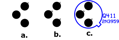 |
Figure 11E |
Figure 11E.a shows three 100-mil round pads placed on a 100-mil grid after the hotspot of a size-20 label has been positioned on the collector pad. The text of the label was changed to c. At this scale, the label is almost too small to read, but often an even smaller label is used.
Figure 11E.b shows two copies of the label were placed over the base and emitter pad and their text changed to b and e, respectively.
Figure 11E.c shows the final result. The footprint has been decorated on layer 255 with an arc and a 3-segment line, and a site and part label have been added.