Drawing Schematics
At this point, you've seen enough that you can probably use HiWIRE® to sketch flowcharts, draw simple schematics, or layout small circuit boards. Normally, you just load component symbols from the various libraries and connect their leads together with lines. If necessary, you could change symbols or even create new ones yourself.
However, HiWIRE® includes a number of facilites that can analyze your drawing and extract useful information such as a netlist (summarizing how components are interconnected) or bill of materials. In order to make use of these facilities, your drawing must follow certain conventions for labeling, grouping and layering.
HiWIRE® schematic libraries assume a grid of 6 mils (0.006 inches) and use two label sizes: 1 (for labels you don't want to see when the drawing is printed) and 7 (for labels you do).
These dimensions aren't really meaningful; schematics are usually scaled to fit the media on which they're rendered. Using a 6-mil grid assures snap is helpful when wiring the components. Size-1 labels are small enough they don't get in your way as you work on your drawing.
Definitions
An electronic system is a collection of interconnected components; each component has two or more terminals or pins. These pins are interconnected with other pins to form nodes or nets.
In a schematic, each physical component is represented by one or more component symbols; its terminals are usually represented by lines, perhaps with annotating labels. Connections between components are represented by other lines, along with dots, used to show connection between crossing lines. These drawing conventions have a long tradition and widespread acceptance.
For example, consider the schematic for the simple electronic system shown below. It has five components, each having two pins: three inductors, and two capacitors.
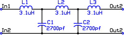 |
Figure 10A |
In its simplest form a netlist is simply a compilation of sets of interconnected pins. The above filter has five nets:
In1 is connected to the left pin of L1.
The right pin of L1 is connected to the left pin of L2 and the top pin of C1.
The right pin of L2 is connected to the left pin of L3 and the top pin of C2.
The right pin of L3 is connected to Out1.
The bottom pins of C1 and C2 are connected to In2 and Out2.
A netlist provides a convenient way to summarize some of the information contained in the schematic: the connections between component pins. It can be used as a starting point for simulating the circuit or creating a circuit-board layout.
Before we discuss HiWIRE's drawing conventions, here are some terms we'll use:
- conducting layer
A drawing layer on which connections may be made. For schematics, HiWIRE always allows connections on layers 0, 1 and 2, but, you may conscript consecutive layers 3, 4, etc., for that purpose.
- insulating layer
A drawing layer greater than the maximum conducting layer. When analyzing your drawing for connections, HiWIRE scans layers 3 and upward to find a layer without conductors. That layer and all higher-numbered layers are presumed insulating.
- conductor
A solid line, arc or connection dot on a conducting layer of your schematic. Polygons, Dotted and dashed lines are not conductors.
- wire
A thin conducting line or arc in a schematic drawing. Wires represent component pins and the individual connections between them. The HiWIRE schematic libraries use 1 mil (0.001") lines for wires. Unless you have a very good reason not to, you should too.
- bus
A thick conducting line or arc in a schematic drawing. Buses reduce clutter by representing multiple similar connections that otherwise would require many individual wires following essentially the same path through the schematic. Buses should be thick enough to be easily visually distinguished from wires. With HiWIRE's schematic libraries, 3-mil lines are best for buses.
- conductor label
A label with no attribute whose hotspot touches a schematic wire or bus. The label must be on a conducting layer, but it can be on a different layer than the conductor. If the label is in a group, the conductor must be part of the same group. That is, a label won't reach outward and touch a conductor outside its own group but will reach inward and touch conductors within nested groups.
- wire label
A conductor label that touches a single wire.
- bus label
A conductor label that touches a single bus, but if a label touches both a single wire and a bus, it is a wire label.
- dot
A pad of any size in a schematic diagram. For 1-mil wires, a 2x2x2 mil pad makes an attractive dot. Dots are used to connect crossing wires. Dots cannot be labeled.
- site label
A label with an attribute of site. Note that site must be spelled exactly as shown, in lower-case letters. It won't do to spell it Site or SITE. Site labels may be placed on any layer and associate a group of objects in a schematic with a particular component in the design.
- drawing component
A group of objects that includes a site label. Although a component can contain nested groups or even other components, its site label must be outside any nested groups. Components may symbolize an actual physical element in the design, or they may represent assemblies of several such elements.
- symbol
A drawing component that includes no nested components. A symbol may contain nested groups, but the groups cannot contain a site label. One or more symbols may used to represent the actual physical elements in your design.
- assembly
A drawing component that includes nested components: either symbols, subassemblies, or both.
- assembly definition
A mechanism to allow a detailed, concrete representation of a recurring fragment in a larger design. Definitions are used when repeating the details would be redundant, monotonous and confusing.
- part label
A label with an attribute of part. Note that part must be in lower case. Part labels may be placed on any layer. They appear in the bill of materials and are used to implement hierarchical schematics.
- functional block
A symbol that contains a part label (as well as a site) but without nested components. It provides an abstract representation of instances of an assembly without the clutter of details in its definition.
- formal definition
A part label, associated drawing components, and the conductors which interconnect them. The part label's text names the definition, and the part label must not be a member of any component. A formal definition is restricted to the members of the group (if any) holding the part label. Connections to the nets of a formal definition from outside its group are forbidden. Formal definitions are advisable when an assembly contains more than a handful of components.
- example
A definition formed by an assembly by including a part name (as well as a site). The part label's text names the definition, and it must not be a member of any nested component. In contrast to a formal definition, certain connections to the nets of an example are allowed. Examples are best restricted to assemblies containing only a few components.
Drawing Conventions
When drawing a schematic, you need only use two layers: 0 and 255. Solid lines and arcs you draw on layer 0 are wires and buses that specify connections between components. Connection dots are then usually placed on layer 0, too.
In contrast, anything you draw on layer 255 is non-conductive. That is, layer-255 lines and arcs are there for ornamentation only; they do not define interconnections. Likewise, dotted and dashed lines do not define connections regardless of their layer. Polygons do not define connections an a schematic drawing.
For example, consider a schematic symbol for a 4009 hex, CMOS inverter, pulled from one of HiWIRE's libraries:
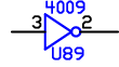 |
Figure 10B |
There is a 3-segment line and a small circle on layer 255 (here rendered in blue) that comprise the well-known logic symbol for an inverter. These two objects are nonconductive and are present in the drawing only for the benefit of a technician trained in reading schematics.
U89 is the site label for this symbol. 4009 is a part label. These labels are on layer 255 by convention, but they could be placed on any layer.
As you may recall, there are five other inverters in the same physical package, but these gates need not be part of the same symbol so long as all share identical site labels: U89.
The two horizontal lines on layer-0 (here rendered in black) are the wires that define the component pins. Two layer-0 conductor labels, 1 and 2, are carefully placed so their hotspots are in the middle of the wires. These two labels name the input and output pins of the symbol.
When HiWIRE analyzes the connections in your drawing, it is primarily concerned with identifying components, their pins, and the connections between them. HiWIRE examines site, part, conductors and conductor labels. While other objects are important for a human viewing the schematic, HiWIRE ignores them entirely.
For example, once the decorations on insulating layers are removed, the filter circuit from Figure 10A looks like this to HiWIRE:
 |
Figure 10C |
Simplified this way, it is easy to recognize the five nets in the circuit.
While many schematics will use only layers 0 and 255, you can use additional layers if you wish. As explained earlier, HiWIRE analyzes connections on layers 0, 1, 2 and any consecutive layers occupied by conductors. You could, for example, use layer 1 to specify critical signals that needs extra attention during circuit-board layout, use layer 2 for power distribution and leave layer 3 empty to signify there are no more conducting layers.
When you print a schematic, you control the display of the various layers. Hence, you can create drawings that have the primary signal connections in a different color, or put manufacturing and test notes on other layers (e.g., 4 through 254. You later decide to include or exclude those layers when you print your schematic for a specific audience.
Connecting with Wires and Dots
In a schematic, HiWIRE considers two wires connected if an end or interior vertex of one wire touches the other. Dots (HiWIRE pads) connect to any wire they touch. They can be used to connect crossing wires that otherwise would not be connected. Arcs have only ends; there is no interior vertex.
It may be helpful to think of schematic wires as being insulated except at their ends and where they bend at an interior vertex. At their ends and elbows, they are honed to a sharp point that can penetrate the insulation of another wire. Imagine dots as covered with metallic thorns that penetrate and connect to any wire they touch.
Figure 10D shows some examples of wires that are connected and not connected:
 |
Figure 10D |
Here, layers 0 (black) and 1 (red) are used so you can clearly distinguish each wire. Normally, all the wires would be on layer 0.
On the left, a three-segment, layer-0 wire twice crosses a two-segment wire on layer 1. A disjoint two-segment, layer-1 wire lies below. The final wire is really three objects: two lines joined to an arc that “hops over” the crossed conductor. This convention is tedious to draw and has largely fallen out of favor with modern designers.
On the right, a three-segment, layer-0 wire is connected to three layer-1 wires. At the top, the connection is by virtue of touching an internal vertex of the three-segment wire. At the bottom, the two-segment wire's end is touching. In the middle, a dot connects two segments that would otherwise just cross.
Since component pins are merely labeled wires, to connect a wire to a pin, simply draw the wire so that its endpoint touches the pin or so that the end of the pin touches the wire.
Be careful when dragging a mid-segment knob to bend a wire. This breaks the segment in two and introduces a new vertex which is impossible to see if the new segments somehow end up colinear. Later, if another wire crosses this hidden vertex, a spurious connection will be made to this vertex.
You can expose the vertices by selecting the wire, but don't be confused by the mid-segment knobs. They are not vertices.
Using Labels to Name Networks
HiWIRE uses labels, specifically site, part and conductor labels to generate names for components and pins for inclusion in the netlist. HiWIRE transforms a drawing label into a netlist name by first discarding leading blanks from the label text and discarding anything following an embedded blank. Fom what remains, HiWIRE discards any characters not included in the following list:
A through Z
a through z
0 through 9
+ – * / $ _ . , !
If there are 32 or more characters left, HiWIRE retains only the first 31. If there are no characters left, HiWIRE disregards the label.
As an example, consider the four drawing labels shown in Figure 10E. The first three labels are equivalent; the generate the netlist name 7400. HiWIRE disregards the last label.
 |
Figure 10E |
In the first two labels, a blank following 7400 causes the remaining text to be discarded. In the third label, (, %, [, ] and ) are discarded. In the fourth label, 7400 follows an embedded blank, so it is discarded. The remaining ( is also discarded; hence this label is ignored by HiWIRE.
Naming Wires
When a wire is labeled with a conductor label, HiWIRE assigns the wire a wire name. If the label is outside any component, the name is simply the netlist name, derived from the label text as described above. If the label is inside a component, the name is a qualified wire name in the form: (site wire), where site is derived from the component's site label(s).
Parentheses distinguish the qualified name from an an unqualified wire name, defined outside of any symbol.
Figure 10F shows a named wire (in red) interconnecting two symbols, an AND gate and an inverting buffer:
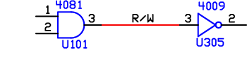 |
Figure 10F |
The connection has three names: (U101 3) , R/W , and (U305 3) . The first and last names are HiWIRE's shorthand for “pin 3 of U101” and “pin 3 of U305”. If asked to list the connections made by these wires, HiWIRE would respond with a parenthesized list that included all the names of the wires:
((U101 3) R/W (U305 3))
Implied Connections
Two conductors with the same name are connected, even if they do not touch.
This convention is used to specify connection between sheets of a multi-sheet drawing; wires with the same name on different sheets are regarded as connected.
Naming wires is also useful to handle large nets such as power and ground. Figure 10G shows a drawing fragment that incorporates groups Vcc and gnd from one of HiWIRE's libraries:
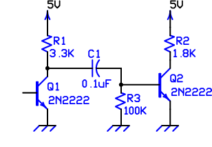 |
Figure 10G |
Vcc is not a component because it contains no site label. It contains only a line, two arcs and a conductor label, 5V. Inside both symbols R1 and R2, the top wires are each labeled with conductor labels a, but both these labels are too tiny to be seen. Somewhere in the netlist we might expect to see:
( ... (R1 a) ... (R2 a) ... 5V ... )
Likewise, gnd is not a component. It contains three diagonal layer-255 lines, two wires, and a label, gNd, too tiny to be seen. Thus, the emitters of Q1 and Q2 and the bottom pin of R3 are all connected to three wires labeled gNd, and HiWIRE determines they are all connected together.
Defining Component Symbols
Often, the easiest way to create a new component is to modify an existing symbol from one of the libraries. For example, the 74AS00 NAND gate on the top right was created from the 7400 gate on its left by simply changing its part label:
 |
Figure 10H |
More extensive changes to an existing symbol can also be made quickly. Drag a copy to an uncluttered area and Edit->Free it. Make the changes and Edit->Bind the result. In the example above, the three-input NAND gate bottom right was created by changing the two-input version on its left by adding another pin and rearranging a few drawing elements.
Starting from Scratch
To define a schematic symbol without modifying an existing one:
First, create a symbolic representation on an insulating layer (usually 255). You can be as creative and artistic as you want during this phase.
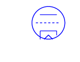 |
Figure 10I |
Second, create a site label (a label with an attribute of site) and place it near your masterpiece so that it is clearly visible. If a part label or other annotation is appropriate, you should also create and place them now.
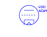 |
Figure 10J |
Third, switch to a conducting layer (usually 0), draw wires to represent the component pins, and label each of them with the name of the pin. Make sure the label's hotspot touches the wire. (This is easiest if you let the labels and wires snap to grid.)
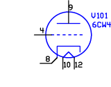 |
Figure 10K |
Finally, switch to layer 0, lasso the pieces, and Edit->Bind them into a full-fledged symbol. Drag the new symbol into position and connect it into your design.
Multi-symbol components
Actually, a physical component may be represented by several schematic symbols that all have the same site name. This property is useful when a single physical component contains multiple independent parts (e.g., a 7400 quad 2-input NAND gate or a 7474 dual D flip-flop).
If multiple symbols are used to represent a single component, make sure their part labels (if any) don't contradict each other. Also make sure that each component pin is defined in only one symbol.
Busing Like Connections Together
When several wires make very similar connections, it is customary to represent them all with a single wide line called a bus. A bus is the schematic equivalent of a multi-conductor cable or wiring harness. In large cables, a color code must be used to identify a particular conductor where it emerges from the bundle. HiWIRE uses a special wire label called a tag to distinguish each member wire in the bus.
Schematic symbols in HiWIRE's libraries use 1-mil lines for wires. We recommend using 3-mil lines for buses to make it easy to distinguish them from the thinner wires.
Exactly like wires, two buses are connected when the end or elbow of one bus touches the other. Mainly for aesthetic reasons, a dot cannot be used to connect two crossing buses. You'll need to devise another way to make the connection obvious. Meanwhile, think of buses as encased in a tough outer sheath that protects the wires inside from a dot's metal thorns.
A wire joins the bus (or emerges from it) if its endpoint touches the bus. Only a wire endpoint will work; an interior vertex cannot join a bus. A bus cannot make a wire join it unless it touches it at one of the wire's ends.
When a bus is labeled using a conductor label, HiWIRE assigns it a bus name. If the label is outside any component, HiWIRE derives the name from the label text as described earlier, and appends [] to distinguish it from a simple wire name.
If the bus label is within a drawing component, the bus has a qualified name in the form: (site bus[]).
Labeling a bus in a schematic component creates a compound pin, primarily useful in the realm of a hierarchical drawing. We'll mostly defer discussing that technique for now.
Wires which join a bus must be tagged so they can be recognized at other locations where they emerge. There are two additonal criteria a wire label must meet to be considered a tag:
The labeled wire must join exactly one bus.
Both the bus and the label must be outside any drawing component (or in a hierarchical drawing, both be within the same component, but outside any nested component).
In mutlti-conductor cables, it's common to parallel two or more wires for extra current-carrying capability. In contrast, in a HiWIRE schematic, a set of touching wires that joins a bus is allowed only one tag. Connections to the set must be either made directly (by touching), or by joining the same bus and having the same tag. Implicit (named) connections are not allowed. By corrolary:
A set of touching wires may only join one bus.
Other than the single tag, no other labels are allowed outside components. (or outside nested components in a hierarchical drawing).
While these rules seem arcane, they turn out to be quite natural in practice. To better understand the concepts, consider the following drawing fragment contrived to test the drawing analyzer:
 |
Figure 10L |
The drawing holds a 5-pin symbol. The blue elements are on a non-conducting layer and, along with the black wires and their names, are members of a drawing component whose site name is U32. Red objects are outside the component: A two-segment bus dangles from a one-segment bus named Tag, a disjoint, anonymous bus hovers below, and five additional wires make connections between component pins and the buses.
Labels 1, 2, 3, and 5 touch exactly one wire each, but the wires don't join any bus. None of these labels are tags.
Label 4 touches a 1-segment wire that has been stretched so it joins the 2-segment bus, but 4 is part of the symbol, and the bus is not. Label 4 is not a tag.
Label a touches a single 3-segment wire, but that wire joins two buses at the point all three touch. Label a is not a tag, and this is an error.
Label b touches both the 2-segment wire and the 2-segment bus. It is thus a wire label, and the one labeled wire joins the two-segment bus. Although it joins a bus at both ends, there's only one bus. Label b is a tag.
Label c touches the same two-segment wire as b, but it also touches the stretched wire defining component pin 3. A label may touch only one wire, so this is an error.
Label d is a valid wire label, not a tag, but it bestows upon its wire the an unqualified name that could foster an implied connection. This is an error.
Labels e both touch the component wire stretched to join the two-segment bus. Both these labels are tags, and even though their text matches, only one tag is allowed. This is an error.
Labels f and g are both tags, but they are members of a 3-wire connected set that includes the component output pin. This is an error.
Label h is the normal case. It touches a single wire joining the two-segment bus at one end and touching the component pin at the other. It's how you'd draw the connection if you weren't trying to test the problematic cases of a-g.
HiWIRE processes the text of the tag as described earlier to derive a bused name for the wire. Wires joining the same bus with matching tags are deemed connected by HiWIRE. If the bus is named, HiWIRE assigns the wires a name that includes both the bus name and the tag.
The full name of the wires takes the form: bus[tag] or (site bus[tag]). The qualified form is used in hierarchical designs when the bus label is inside a drawing component.
For example, consider the following drawing fragment:
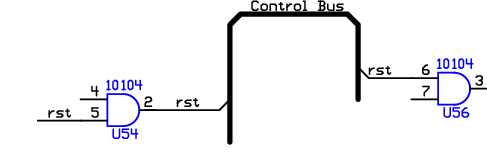 |
Figure 10M |
The fragment shows three names for the wires that joins the bus: (U54 2) , (U56 6) , and Control[rst] . If the bus were not labeled, the wires lose their last alias since there is no bus name from which to construct it.
Also notice an input to U54 is connected to a wire labeled rst, but since this wire does not join the bus, HiWIRE does not infer a connection to the bused wire. Two names for the wire connected to pin 5 of U54 are (U54 5) and rst.
Two buses are connected if they have the same bus name (or qualified bus name) even though they do not touch. This convention may be used to specify connections across sheets of a multi-sheet drawing.
Extracting a Netlist
To extract a nelist from your schematic drawing, the analyzer script will infer the number of conducting layers, but you need to explicitly and carefully:
Specify the maximum wire width. Wider lines will be treated as buses. If you used the components from the HiWIRE library and followed the admontion to interconnect them using 1-mil (0.001") lines for wires, then that is the value you should specify.
Select the portion of your drawing to be used for the netlist. For example, you may want to keep your schematic and PCB in the same file. That's fine, but you must always layer-0 lasso the schematic portion before attempting to analyze it. Conversely, if your schematic is in a drawing by itself, you must either lasso it all or shift-click to make sure nothing is selected.
A common mistake is to attempt to extract a netlist when you've made a change that left a single symbol, label or wire selected. The analyzer will quickly extract a netlist, but it will be quite a bit shorter than you expected.
It may help to print out the following section to use as a checklist each time.
Step by Step
If it's not already displayed, Edit->Preferences… to display the dialog, and set Line Width: to 1 mil (or specify the widest line you used to draw wires).
Lasso select the portion of your drawing to analyze, or click-select nothing to use it all.
Select Script->Extract a netlist…".
In the dialog, specify the name of the file that will hold the netlist, and yada, yada, yada.